Wire-to-wire: TSVs may be the key to faster semiconductors
Wire-to-wire: TSVs may be the key to faster semiconductors
TSVs are very thin copper wires, typically 5 microns in diameter (roughly a tenth the thickness of a human hair). Arranging these wires in an array between stacked silicon chips enables extremely fast communication between them, and thus extremely high bandwidth and fast processing. But it comes at a cost.
“One of the biggest challenges in advanced 3D packaging is dealing with heat,” said Shuhang Lyu, a Ph.D. student in mechanical engineering. “The high density of materials so close together generates more heat than traditional 2D chips. The physical materials start to strain and crack, which affect performance and reliability.”
In other words, you can’t make chips faster by simply shrinking the TSVs and adding more of them. The physical materials (the copper of the wires and the silicon of the chips) encounter problems as they interface together, heat up, and begin to push and pull on one another. The problem gets even more difficult as the wires get smaller — heating problems intensify, and their elasticity changes as they shrink.
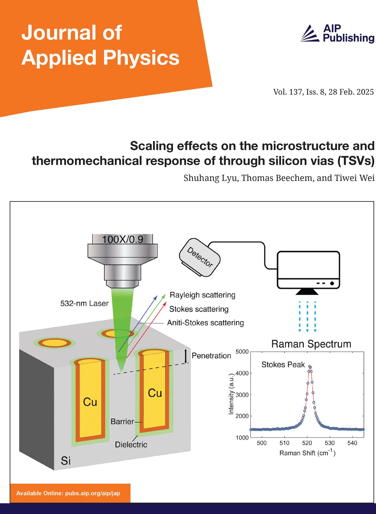 Lyu’s research into this interaction between TSVs and silicon has been highlighted on the cover of the Journal of Applied Physics.
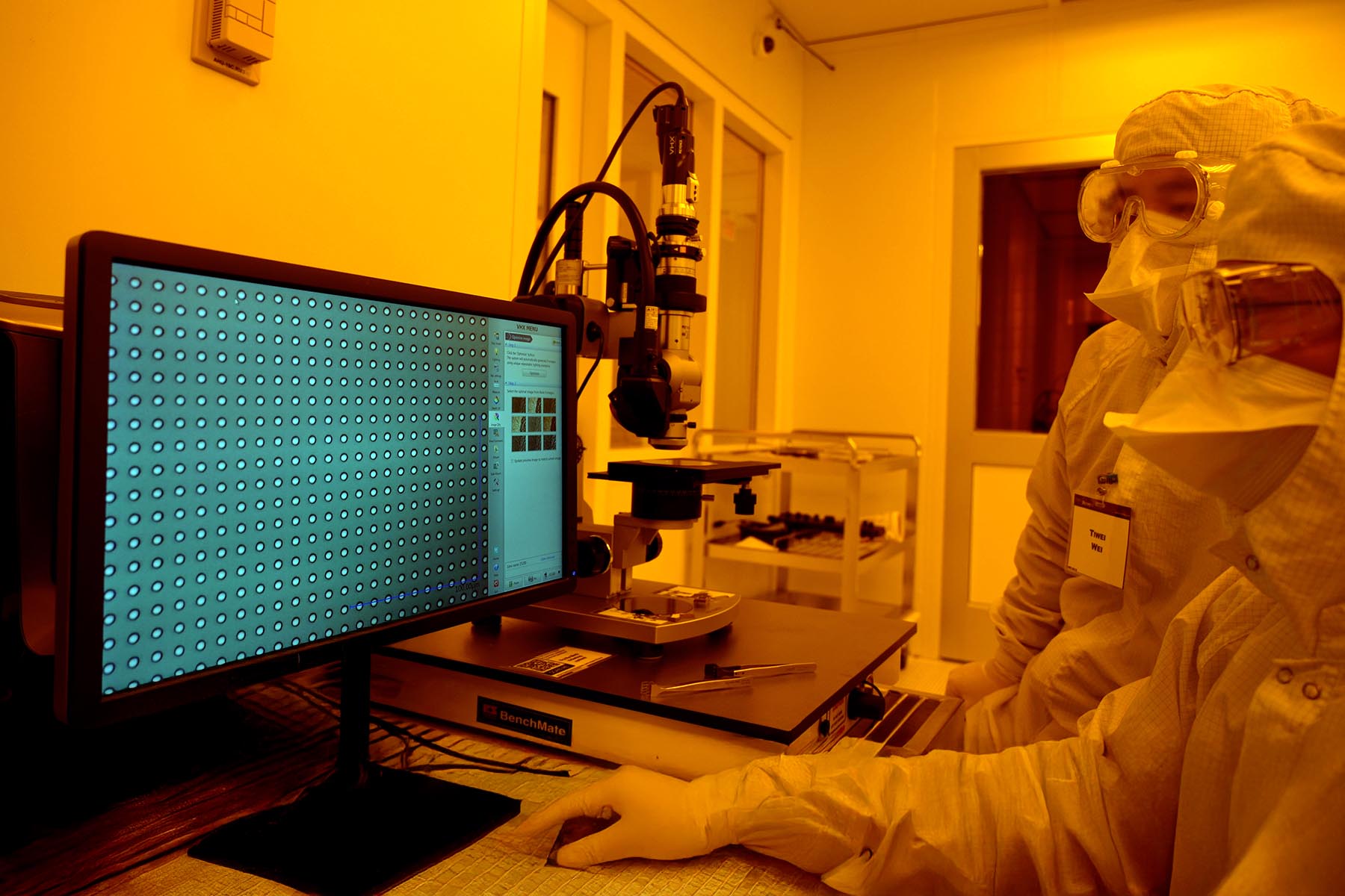
To study thermomechanical stress and strain at these microscopic scales, Lyu first had to construct prototypes. He built sample silicon wafers with arrays of TSVs of different diameters: 4 microns, 2 microns, and 1 micron. This was accomplished at Birck Nanotechnology Center, a massive cleanroom facility at Purdue that focuses on the manufacture and characterization of semiconductors.
Then Lyu studied the thermomechanical properties of the samples using a combination of tools. “We used Raman spectroscopy and scanning electron microscopy to study the microstructure of the TSV. We found that as the TSV shrinks down, the copper’s microstructure changes significantly.”
Like most materials, copper has a grain structure. Lyu discovered that at smaller and smaller sizes of TSV, the copper grains themselves also become smaller. This changes their elastic response, suggesting that TSVs might actually become stronger as they shrink in size.
Lyu is co-advised by Tiwei Wei, assistant professor of mechanical engineering; and Thomas Beechem, associate professor of mechanical engineering. They both study heat transfer and thermomechanical response at the microscopic scales of semiconductors. Purdue’s growing semiconductor innovation ecosystem is one of the key pillars of Purdue Computes, a comprehensive initiative across computing departments, physical AI, semiconductors, and quantum science and engineering to enable unparalleled excellence at scale.
“The fundamental reason we study these material properties is to make semiconductors better in the future,” Lyu said. “Microscopic stress and strain is directly related to the performance of the device. If chip manufacturers can use our models to improve their designs and materials, then semiconductors will become much faster and more reliable.”
Source: Shuhang Lyu, lyu129@purdue.edu
Writer: Jared Pike, jaredpike@purdue.edu, 765-496-0374
Scaling effects on the microstructure and thermomechanical response of through silicon vias (TSVs)
Shuhang Lyu, Thomas Beechem, and Tiwei Wei
https://doi.org/10.1063/5.0252921
ABSTRACT: The dimensional scaling of through silicon vias (TSVs) is critical for the advancement of high-density 3D integration in future logic-on-logic and logic-on-memory computing architectures. Realizing such scaling demands an understanding of the thermomechanical response at the relevant length scales as both the microstructure and properties of the copper making up the majority of the TSV are dependent upon the size. In response, we examine here the residual stress development of the surrounding Si and microstructural evolution of Cu within TSVs as they are scaled from 5 to 1 μm diameter and thermally annealed. Using a combination of Raman spectroscopic and electron backscatter diffraction imaging accompanied by thermomechanical modeling, a non-monotonic trend between equivalent stress and TSV diameter is revealed. The non-monotonic trend is interpreted using an elastic thermomechanical model that accounts for competition between the global bending of the wafer and local Cu shrinkage. The elastic behavior is attributed, in large part, to a decrease in the mean grain size of Cu—and the accompanying increase in strength—that occurs with reduced TSV diameter. Thus, given the consistency of measured stress with the elastic model and the improved mechanical strength with decreased grain size, annealed Cu TSVs are deduced to remain more elastic compared to their larger counterparts as they scale from 5 to 1 μm.